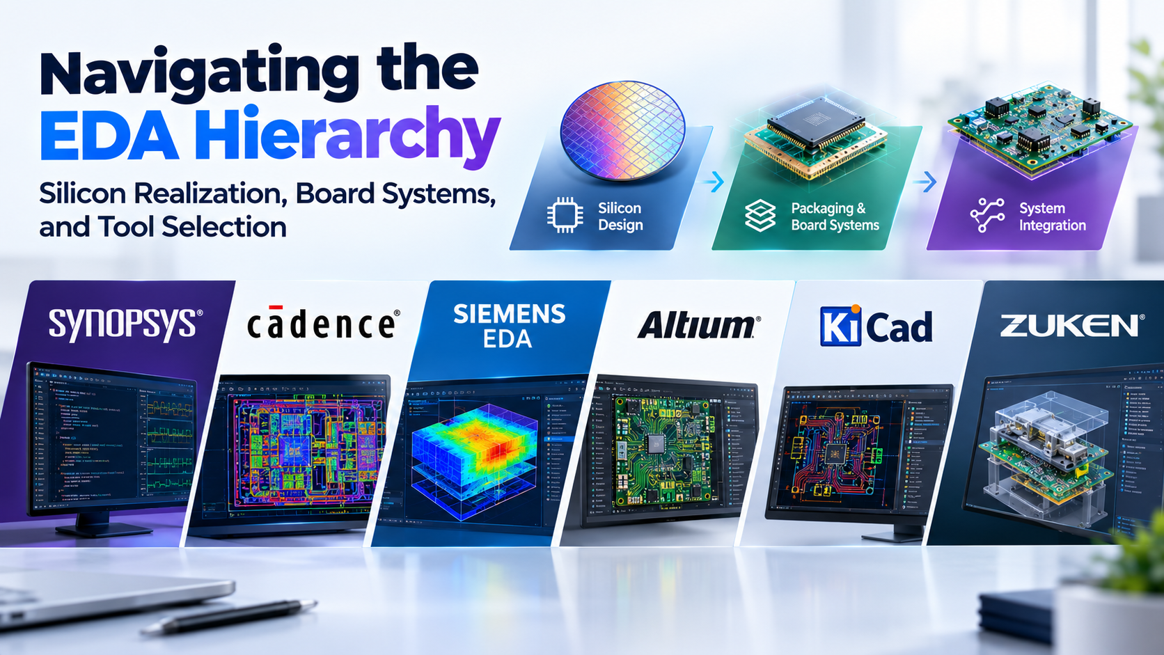
Modern microelectronics has outpaced the limits of human spatial reasoning. A cutting-edge system-on-chip (SoC) packs tens of billions of transistors into a sliver of silicon the size of a fingernail. Interconnect lines measure a fraction of the width of a virus, and switching speeds trigger high-frequency electromagnetic parasitics that turn simple wires into complex transmission lines. Designing these systems directly by hand is impossible.
Electronic Design Automation (EDA) software provides the computational backbone that makes modern electronics viable. It spans the toolchains that transform high-level behavioral algorithms, register-transfer level (RTL) code, and system schematics into physical, validated semiconductor masks and printed circuit assemblies.
Yet evaluating and selecting EDA tools presents a structural trap. EDA is not a single market category, but an interdependent stack of specialized sub-disciplines. Procuring an enterprise-tier IC physical verification engine when a team simply requires advanced packaging layout, or adopting a low-overhead PCB tool for a high-speed memory interface design, introduces project-threatening friction.
Understanding EDA requires dissecting its architectural layers: where software boundaries sit, how data moves across abstraction levels, and where the engineering risks lie.
The Three Fundamental Domains of EDA
The EDA landscape divides into three operational tiers based on the scale of physical physics being managed: digital and system-level IC design, analog and custom silicon, and systems-level PCB design.
1. Front-End Logic and Digital Verification
This domain operates primarily in code and state logic. Engineers express design intent using Hardware Description Languages (HDLs) such as SystemVerilog, VHDL, or modern frameworks like Chisel.
- The Core Task: Verify architectural intent before generating physical transistors. This involves high-throughput logic simulation, formal mathematical verification, and static timing analysis (STA).
- Failure Modes: Functional bugs that escape logic verification cost orders of magnitude more to correct after tape-out. At the same time, verification often consumes more compute cycles and engineering hours than the design phase itself.
2. Back-End Silicon Implementation and Physical Verification
Once logic is frozen, synthesis tools translate behavioral RTL into structural gate-level netlists mapped to a specific semiconductor foundry’s standard-cell library.
- The Core Task: Place-and-route engines arrange billions of logic gates, construct balanced clock trees, and route metal interconnects across dozens of lithographic layers. The design must then pass Design Rule Checking (DRC) and Layout Versus Schematic (LVS) verification against the foundry’s Process Design Kit (PDK).
- Failure Modes: Timing closure issues, electro-migration, IR-drop (voltage sagging), and thermal hot spots. If the physical layout deviates from the mathematical models provided by the foundry, the produced wafer will suffer fatal yield collapse.
3. Board-Level and Packaging Systems (PCB & Advanced Packaging)
Physical dies must be mounted, powered, and interconnected on substrate packages and printed circuit boards.
- The Core Task: Managing the electrical, thermal, and mechanical boundaries between discrete integrated circuits, passive components, power supplies, and external interfaces.
- Failure Modes: Signal integrity degradation (crosstalk, reflection, jitter), poor power distribution impedance, thermal throttling, and electromagnetic interference (EMI) failing regulatory certification.
Primary EDA Platforms Across the Hardware Lifecycle
The commercial EDA market exhibits deep structural consolidation. A small triad of enterprise vendors commands the silicon synthesis and signoff space, while specialized players and an evolving open-source ecosystem support niche, rapid-prototyping, and academic development.
| Platform / Vendor Suite | Primary Operational Layer | Architecture & Delivery | Primary Strength | Structural Trade-off |
| Synopsys (Design Compiler, IC Compiler II, PrimeTime) | Digital IC Synthesis, Place & Route, Golden Timing Signoff | Linux-native workstation & compute cluster; hybrid cloud | Defacto industry standard for digital synthesis and golden static timing verification | Massive total cost of ownership; extreme learning curve requiring dedicated CAD teams |
| Cadence (Virtuoso, Innovus, Allegro) | Custom Analog/Mixed-Signal, Digital Implementation, High-Speed PCB | Linux/Unix cluster (Silicon), Windows/Linux (PCB) | Unrivaled standard for analog/RF layout (Virtuoso); seamless multi-layer constraint management | Fragmented UI paradigms across legacy acquired tools; complex multi-tier licensing |
| Siemens EDA (Calibre, Xpedition) | Physical Verification (DRC/LVS), Enterprise System Packaging | Linux compute grid (Verification), Windows/Linux (Systems) | Universal foundry signoff benchmark (Calibre); deep multi-board electromechanical co-design | High deployment complexity; requires rigorous internal administration to maintain rules |
| Ansys (RedHawk-SC, HFSS, SIwave) | Multiphysics, Thermal, Power Integrity, 3D Full-Wave EM | Linux/Windows high-performance computing (HPC) | Precision multiphysics modeling of electromagnetic and thermal interactions | Purely an analysis/verification layer; relies entirely on external authoring tools for source geometry |
| Altium Designer | Mid-Tier to High-Complexity Commercial PCB Systems | Desktop-centric Windows application with cloud data services | Highly unified schematic-to-3D-PCB workflow with integrated component supply intelligence | Not architected for leading-edge silicon package design; heavy local hardware demands |
| Open-Source Stacks (OpenROAD, Magic, KiCad) | Academic IC Realization, Open-Hardware, Small-Scale PCB | Cross-platform, CLI-driven, containerized Linux environments | Zero license friction; Git-native version control; programmatic scripting flexibility | Minimal native support for advanced deep-submicron foundry nodes; no enterprise liability support |
Architectural Breakdown: Where Tools Diverge
Silicon Implementation: The Synopsys and Cadence Duopoly
For standard digital cell implementation, Synopsys and Cadence maintain an effective duopoly at advanced nodes. The primary differentiator between them rarely comes down to a single headline feature; instead, it centers on timing closure convergence and foundry certification.
HDL (SystemVerilog)
       │
       ▼
Logic Synthesis ────────► [Design Compiler / Genus]
       │
       ▼
Place & Route   ────────► [IC Compiler II / Innovus]
       │
       ▼
Physical Verification ──► [Calibre / IC Validator / Pegasus]
       │
       ▼
GDSII / OASIS (Tape-Out to Foundry)
In digital flows, Synopsys holds a dominant position in static timing analysis. Its PrimeTime platform is the accepted “golden” timing signoff tool for global foundries. A design is generally not accepted for fabrication by contract foundries until it achieves timing signoff through an approved flow.
Conversely, Cadence Virtuoso serves as the undisputed benchmark for custom analog, RF, and mixed-signal design. While digital design relies on abstraction layers that synthesize code into gates automatically, analog design requires manual, transistor-level drawing of geometry to balance noise, gain, and thermal stability. Virtuoso’s design environment, tightly integrated with the Spectre simulation engine, provides the precise parametric control required to hand-craft analog building blocks.
The Verification Barrier: Siemens Calibre
While both Synopsys and Cadence offer proprietary physical verification engines, Siemens EDA (formerly Mentor Graphics) holds a uniquely protected position with Calibre.
Calibre is the global semiconductor industry’s baseline standard for:
- Design Rule Checking (DRC): Ensuring billions of drawn polygons meet hundreds of geometric constraints imposed by advanced lithography (such as fin field-effect transistor fin spacing and multi-patterning masks).
- Layout Versus Schematic (LVS): Confirming that the physical polygons laid down on the mask correctly represent the intended electrical circuit diagram.
Foundries publish their official PDK rule decks directly formatted for Calibre syntax. While chip designers may use internal tools during active routing, the final tape-out signoff run almost universally runs through Calibre to eliminate disputes between the designer and the fabrication plant.
The System-Level Shift: Advanced Packaging and Multiphysics
Moore’s Law—the predictable cadence of shrinking planar transistors every two years—has encountered physical and economic walls. In response, the semiconductor industry has shifted focus toward heterogeneous integration and chiplets. Rather than printing a massive monolithic die, designers break functions down into smaller dies (compute, memory, I/O) manufactured on different process nodes and stack them on a shared silicon interposer using through-silicon vias (TSVs).
This shift changes the demands placed on EDA software:
- Tool Convergence: Traditional IC tools stop at the chip boundary, while traditional PCB tools cannot handle the sub-micron scale of silicon interposers. Tools like Cadence Allegro Package Designer and Siemens Xpedition Substrate Integrator bridge this gap.
- Thermal and Power Stress: Stacking silicon blocks vertically concentrates heat. High-performance computing engines like Ansys RedHawk-SC and HFSS calculate dynamic voltage drop (IR drop), electro-migration, and radio-frequency resonance across complex three-dimensional structures.
- Shift to Multiphysics: Parasitic extraction can no longer be abstracted as simple RC (resistance-capacitance) trees. It now requires full-wave 3D electromagnetic field solvers that process thermal dispersion, mechanical stress, and signal propagation concurrently.
Open-Source EDA: Viability Versus Production Reality
The open-source EDA domain has evolved from academic curiosities into capable, reproducible toolchains. The primary catalyst was the emergence of the open-source RISC-V instruction set architecture, alongside initiatives like the DARPA OpenROAD project and community-driven, open PDK releases from commercial foundries.
+------------------------------------------------------------------+
|                    The Open-Source EDA Stack                     |
+------------------------------------------------------------------+
| Architecture & HDL    : SystemVerilog, Amaranth, Chisel          |
| Logic Synthesis       : Yosys Open SYNThesis Suite               |
| Static Timing Analysis: OpenSTA                                  |
| Place & Route         : OpenROAD, Graywolf                       |
| Layout & DRC/LVS      : Magic, KLayout, Netgen                   |
| Board-Level Systems   : KiCad                                    |
+------------------------------------------------------------------+
Where Open Source Works
Open-source stacks excel in rapid algorithmic exploration, academic instruction, and the design of cost-sensitive IoT silicon manufactured on mature micro-scale lithography nodes (such as 130nm down to 28nm planar processes).
Because tools like Yosys and OpenROAD operate cleanly via command-line interfaces and Python/Tcl scripts, they can be embedded directly into modern software-style continuous integration (CI) workflows. Every code commit to an RTL repository can automatically synthesize, place, route, and report power-performance-area (PPA) metrics without licensing friction or cloud credential bottlenecks.
The Boundaries of Production Viability
Open-source silicon tools encounter severe barriers when confronting sub-16nm FinFET or gate-all-around (GAA) architectures:
- PDK Licensing and Non-Disclosure Agreements: Leading-edge foundries protect their proprietary physical manufacturing data under strict legal NDAs. Open-source tools cannot natively distribute rule decks for competitive commercial nodes without compromising the foundry’s trade secrets.
- Computational Scale: Routing tens of billions of nets across 15+ metal layers requires advanced distributed multi-threaded solvers. Proprietary engines have absorbed decades of optimization that open-source tooling cannot match for ultra-dense layouts.
- Absence of Legal Indemnification: If an unhandled edge case in an open-source synthesis engine introduces a race condition that ruins a production mask run, the financial loss rests entirely on the engineering company. Commercial EDA vendors charge significant fees partly to provide engineering support and verified signoff credibility.
Evaluating Total Cost of Ownership
Investing in an EDA stack involves cost structures fundamentally different from standard enterprise enterprise-resource-planning (ERP) or product-lifecycle-management (PLM) software.
Licensing Paradigms
Silicon-level EDA licensing is heavily consolidated around Term-Based Licenses (TBLs). A license grants access to software modules for a fixed window (typically two to three years).
- Feature Tokenization: Core solvers are often sold alongside floating “tokens.” Running an analog circuit simulator on 8 cores requires a base license; distributing that same run across 128 cores to accelerate characterization consumes an escalating ladder of compute tokens.
- Flexibility vs. Predictability: Vendors bundle portfolios, trading discounts on lesser-used digital verification tools to secure long-term exclusivity for their flagship layout and synthesis engines.
Compute Infrastructure Costs
The software license is rarely the sole expense. Modern back-end place-and-route, physical verification, and 3D electromagnetic simulations demand massive high-performance computing (HPC) clusters:
- Terabytes of high-speed Error-Correcting Code (ECC) RAM per node to map multi-gigabyte flat layout geometries.
- Ultra-low-latency NVMe-based network file systems to support rapid I/O during extraction and verification steps.
- The administrative overhead of queuing engines like Slurm or LSF to manage cluster utilization across distributed teams.
Switching Costs and Ecosystem Lock-In
The most potent hidden cost in EDA is custom automation and institutional memory. Silicon design firms develop extensive codebases written in Tcl, SKILL (Cadence), or Scheme to automate everything from basic pad ring generation to complex timing closure loops.
Migrating a team from Cadence Virtuoso to an alternative environment does not merely mean training engineers on a new interface; it requires rewriting thousands of internal, battle-tested productivity scripts and re-characterizing verified internal IP blocks.
Practical Selection Guidelines
Navigating the EDA procurement process requires matching the complexity of the physical problem to the minimum viable administrative overhead:
- For Turnkey Commercial Board-Level Hardware: If your primary focus is producing multi-layer embedded systems, IoT devices, or industrial compute modules under tight deadlines, prioritize unified environments like Altium Designer. Its native 3D component-clearance checking and live component distributor links streamline prototype handoffs.
- For High-Density, High-Speed Computing Platforms: If you are engineering complex server architectures, multi-gigabit interfaces (PCIe Gen 5/6, DDR5), or automotive control modules, deploy Cadence Allegro. Its strict Constraint Manager provides the systematic rule enforcement needed to govern complex signal and power integrity regimes across teams.
- For Analog, RF, and Power Semiconductor Development: If your team is building custom integrated circuits, mixed-signal sensor interfaces, or power management ICs (PMICs), Cadence Virtuoso paired with foundry-certified simulation engines remains the industry standard.
- For Multi-Million Gate Digital ASICs and SoCs: If you are building high-performance processing hardware, neural processing units (NPUs), or high-throughput network fabrics, the combination of Synopsys Design Compiler / PrimeTime for synthesis and timing closure, alongside Siemens Calibre for physical DRC/LVS, represents the lowest-risk path to commercial foundry yield.
- For Open Hardware, Research, and Academic Silos: If licensing friction or software-style continuous integration is your operational focus—and your targets are mature planar nodes or educational test chips—the combination of OpenROAD, Yosys, and KiCad delivers genuine engineering autonomy without recurring seat subscriptions.
Strategic Implementation Takeaway
EDA software should never be procured based on generic platform demonstrations or high-level feature matrix comparisons.
Before committing capital to an EDA environment, assemble a rigorous evaluation: take your design team’s most technically demanding sub-circuit—an irregular high-speed routing channel, an analog gain stage, or a dense placement block—and execute a complete verification cycle through to DRC/LVS signoff. The toolchain that converges on timing closure and layout validation with the fewest custom engineering workarounds is the one that will protect your operational capital and safeguard your release schedules.
